3.13.4.2 - Non-Inverting Amplifiers
Apply the non-inverting gain equation without losing its added 1. Identify the feedback junction, choose resistors and output limits, and explain why a voltage follower can preserve a sensor signal even though its voltage gain is one.
The Non-Inverting Feedback Circuit
A non-inverting amplifier receives its signal directly at the input. The input is connected to a junction between , which leads to the output, and , which leads to ground.
[DIAGRAM: asset_name: E.4.2 - Non-Inverting Amplifier Configuration - Diagram 1; asset_slug: E.4.2 - Non-Inverting Amplifier Configuration - Diagram 1; caption: Non-inverting amplifier: Rf and R1 meet at the inverting input; description: Non-inverting amplifier: Rf and R1 meet at the inverting input.]
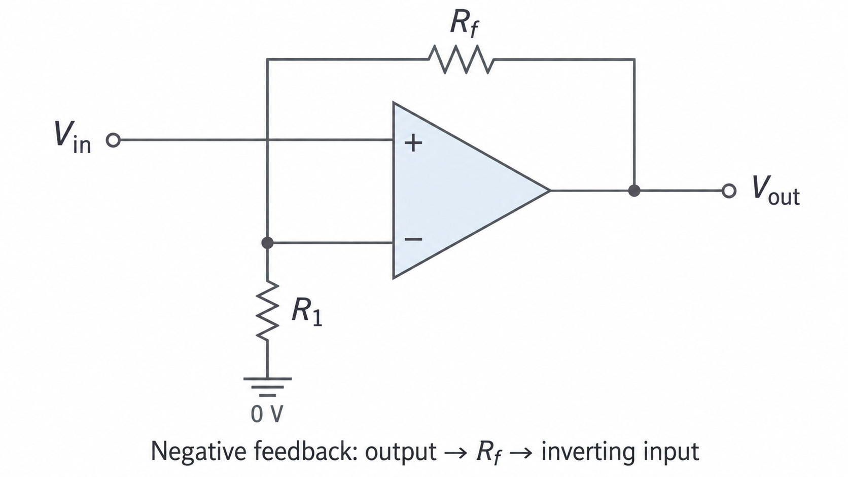
Connection dots mark electrical joins. In this diagram the input wire crosses the feedback wire without a dot, so those two wires are not connected. Both supplies are omitted for clarity; the op-amp still needs power.
If the output rises too far, the divider raises the input above the signal at the input. The op-amp then reduces its output. This negative feedback holds the two input potentials nearly equal during linear operation. Unlike the grounded input in an inverting amplifier, here both input terminals follow the signal: the input is not generally a virtual earth.
The source connects to the op-amp's very high input resistance, so it supplies negligible input current. The output supplies the load current using energy from the power rails. Negative feedback stabilises the gain within the device's voltage and frequency limits; it cannot prevent saturation for an arbitrarily large input.
Applying the Non-Inverting Gain
The closed-loop gain is positive, so a signal keeps its polarity in the linear low-frequency regime.
Non-inverting voltage gain
is always the output-to-junction resistor and the junction-to-ground resistor. AQA writes this lower resistor as in the specification; either label denotes the same role. Identify resistors by connections rather than position on the page. Derivation is not required for this configuration.
With and , . An input of gives ; an input of gives . The resistor units cancel when they are the same.
Since ordinary positive resistors make , this configuration has gain greater than one, approaching one as the feedback fraction approaches unity. It cannot provide a linear low-frequency gain of . A voltage follower is the limiting gain-one arrangement.
Resistor Design and Output Limits
Choosing a non-inverting gain requires the resistor ratio to be one less than the gain:
Continue this lesson.
You’re previewing NovaLearn without an account. Create a free account to read the rest.
Create free account