3.12.2.6 - Electron microscopes
A short electron wavelength helps a TEM reveal fine internal structure, while an STM uses tunnelling to map a conducting surface. Calculate the wavelength scale first, then distinguish it from the practical requirements and limits of each instrument.
Resolution is more than magnification
Resolving power is the ability to distinguish closely spaced features as separate. A smaller minimum resolvable distance means better resolving power. Magnifying an unresolved blur only makes the blur larger; it does not reveal extra detail.
Diffraction limits wave-based imaging. Visible light has wavelengths of a few hundred nanometres, so an ordinary optical microscope cannot separate features on a typical atomic scale of about . Electrons accelerated through a voltage can have a much shorter de Broglie wavelength. This gives a TEM the potential for much better resolution.
Wavelength is one limit, not a guarantee of achieved resolution. Lens imperfections, beam energy spread, scattering and stability also matter. An STM has a different source of sensitivity: tunnelling current changes extremely strongly with tip-to-surface separation. It is not simply an optical microscope with shorter-wavelength illumination.
How a TEM forms an image
A transmission electron microscope sends electrons through a very thin specimen and uses magnetic lenses to form a magnified image. The image contains information about structure within that thin specimen, projected along the beam direction; it is not automatically a three-dimensional view.
[DIAGRAM: asset_name: D.2.6 - Electron Microscopes - Diagram 1; asset_slug: D.2.6 - Electron Microscopes - Diagram 1; caption: The TEM component sequence prepares, transmits, focuses and magnifies the electron beam; description: Scientific teaching diagram with geometry and labels checked against the owning explanation.]
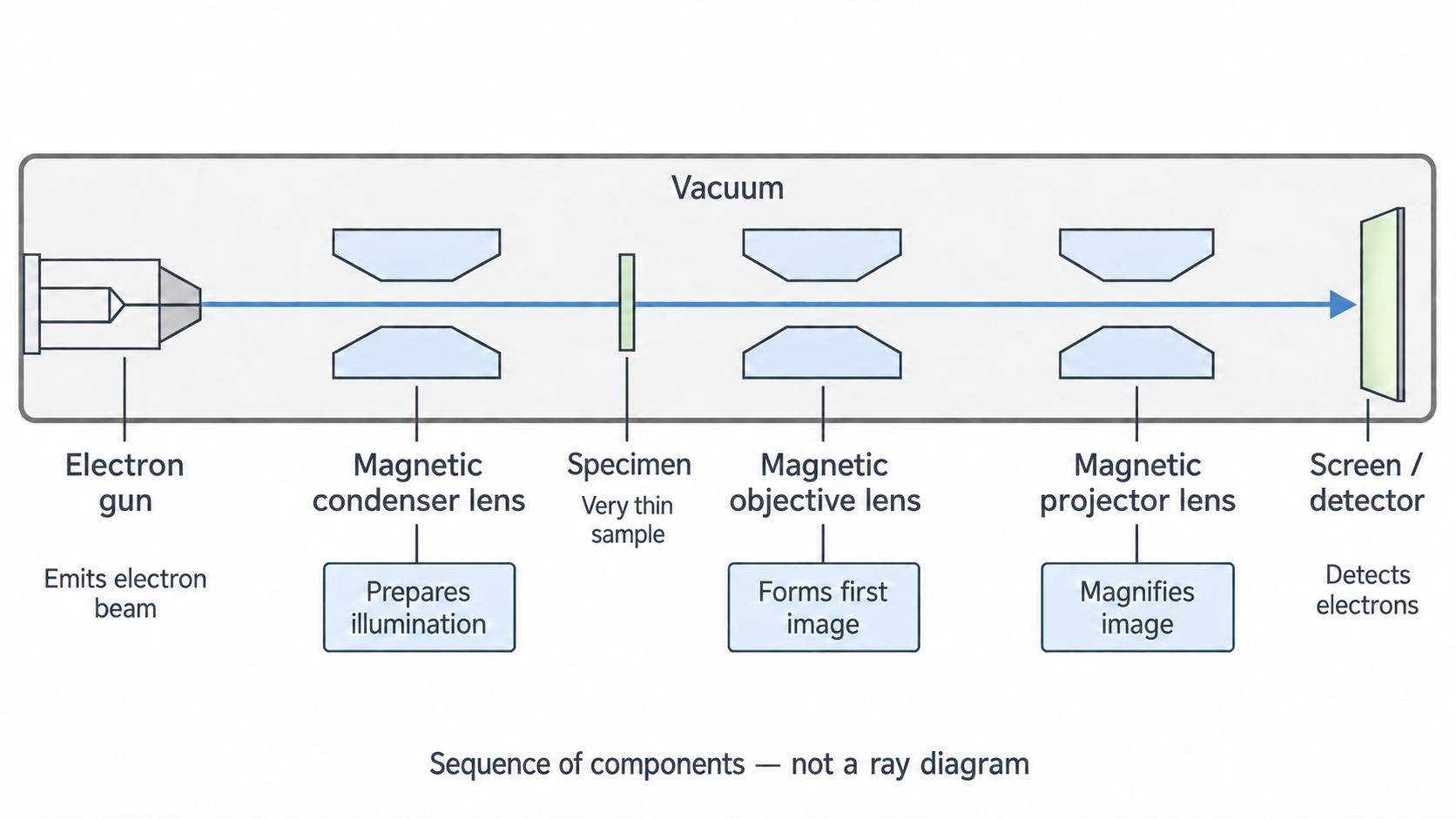
The electron gun emits electrons, for example by heating a cathode, and accelerates them towards a positive anode. The condenser lens controls the illumination reaching the specimen. The specimen scatters electrons differently at different positions. The objective lens forms the first image from electrons emerging from the specimen, and the projector lens magnifies it onto a fluorescent screen or electronic detector. Magnetic fields deflect moving electrons; glass lenses are not used to focus this beam.
The column is evacuated to reduce scattering by gas. The specimen is very thin to allow useful transmission and reduce multiple scattering. A thick specimen may absorb or scatter away much of the useful beam, mix information through multiple scattering, and produce inelastic energy losses. These reduce image clarity. The primary problem is not simply that every electron slows down by the same amount.
Electrons with different energies are focused differently by magnetic lenses, causing chromatic aberration. Energy spread may arise at the source or from inelastic scattering in the specimen. Other lens aberrations and mechanical drift can also limit resolution. A smaller incident wavelength therefore cannot, on its own, promise a perfectly sharp atomic image.
An atomic-scale voltage estimate
To estimate the voltage for an electron wavelength of atomic dimensions, combine with the non-relativistic energy relation . Rearranging gives
For an atomic-size estimate , use , and :
About gives the required wavelength scale. This is an order-of-magnitude estimate, because atomic dimensions are approximate. It does not say that a practical TEM operating at that voltage will resolve individual atoms. Electrons also need to penetrate the specimen, and shorter wavelengths can help reduce diffraction limitations while other imperfections remain.
The squared wavelength is important: halving the target wavelength requires four times the voltage. The equation assumes acceleration from rest without significant loss and . At the much higher voltages of many practical TEMs, electron speeds become large enough that relativistic corrections are needed. Do not present the low-speed formula as an exact high-voltage instrument calibration.
Continue this lesson.
You’re previewing NovaLearn without an account. Create a free account to read the rest.
Create free account