4.6.4.1 - Logic gates and truth tables
Logic circuits turn binary inputs into decisions, arithmetic and stored state. Learn to interpret standard gate symbols, construct truth tables and expressions, follow half- and full-adders, and explain how an edge-triggered D-type flip-flop stores one bit.
Standard gates and their truth tables
A logic gate applies a defined Boolean operation to inputs that each have one of two values.
Boolean value
A value with two possible states, normally represented as 0 and 1, or false and true. A truth table lists the output for every possible combination of inputs.
For two independent inputs there are combinations. Use a consistent order, 00, 01, 10, 11, so no row is missed. NOT has one input and therefore two rows.
| A | NOT A |
|---|---|
| 0 | 1 |
| 1 | 0 |
| A | B | A AND B | A OR B | A XOR B | A NAND B | A NOR B |
|---|---|---|---|---|---|---|
| 0 | 0 | 0 | 0 | 0 | 1 | 1 |
| 0 | 1 | 0 | 1 | 1 | 1 | 0 |
| 1 | 0 | 0 | 1 | 1 | 1 | 0 |
| 1 | 1 | 1 | 1 | 0 | 0 | 0 |
AND is 1 only when both inputs are 1. OR is inclusive: at least one input is 1, including the case where both are 1. XOR (exclusive OR) is 1 when the two inputs differ. NAND is NOT of AND, and NOR is NOT of OR; negate the final gate result, not each input separately.
[DIAGRAM: asset_slug: logic-gate-symbols; description: The six distinctive gate symbols and their output sequences for all input combinations.]
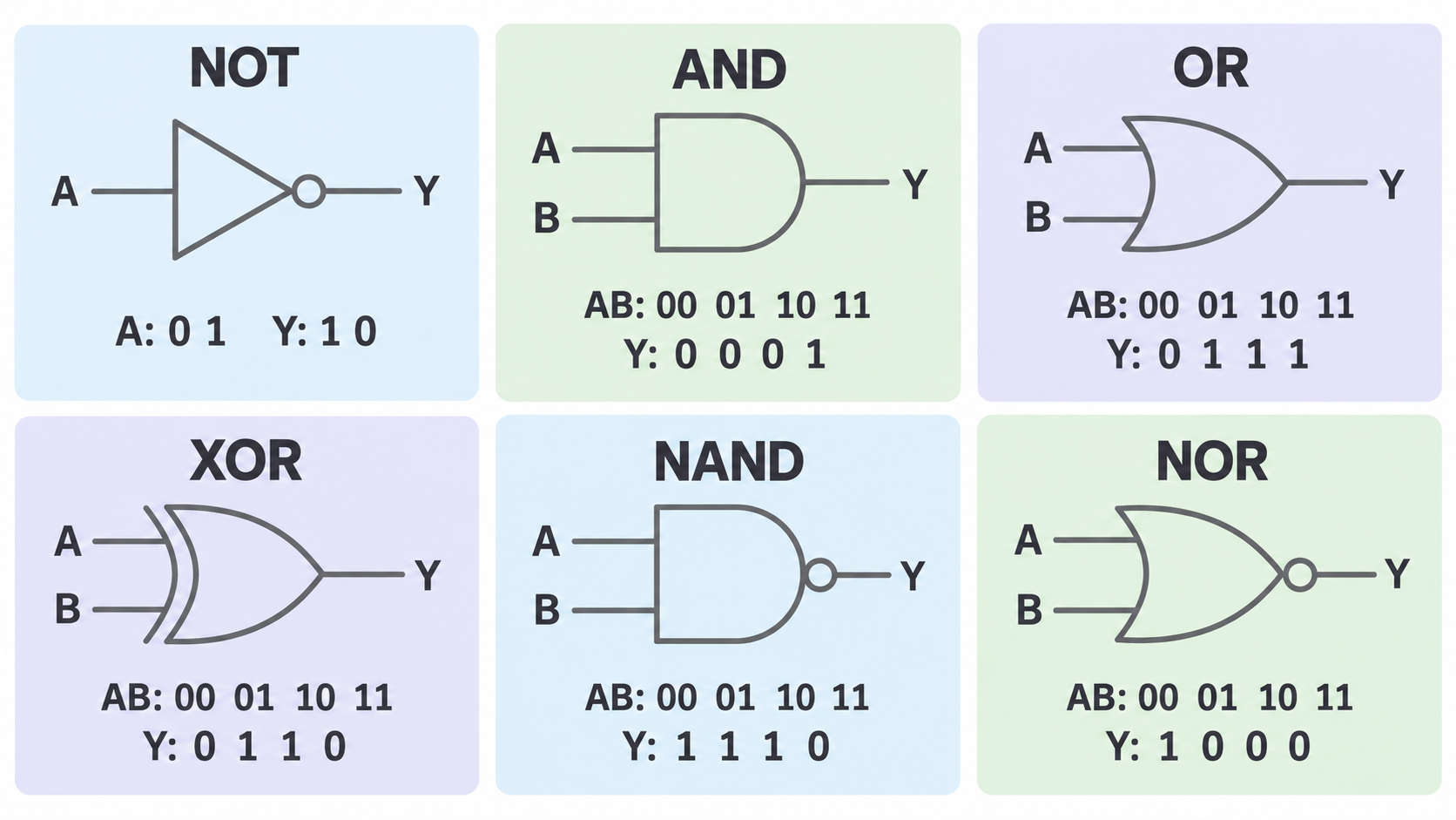
Know the ANSI/IEEE distinctive-shape symbols shown here. NOT is a triangle with a small output inversion circle. AND has a flat input side and curved output side. OR has a curved input side and pointed output; XOR adds a second curved line on the input side of the OR shape. NAND and NOR use their underlying AND/OR shape with an output inversion circle. Input and output lines show connectivity; the little circle means logical inversion and is not a wire junction.
From a connected circuit to an expression
Follow the connections and evaluate intermediate outputs before deciding the final result of a multi-gate circuit.
Label each intermediate wire and work from inputs towards outputs. Suppose A and B feed an AND gate whose output is X; C feeds a NOT gate whose output is N; X and N feed an OR gate whose output is Y. Then
Here means AND, means OR and a bar means NOT of exactly the expression under it. Boolean OR is not ordinary arithmetic addition: in this notation. Parentheses or the bar's extent keep grouping clear. XOR can be written , so has a different meaning from .
With three independent inputs there are rows. Add intermediate columns so a single gate's operation can be checked separately from the final answer.
| A | B | C | X = A AND B | N = NOT C | Y = X OR N |
|---|---|---|---|---|---|
| 0 | 0 | 0 | 0 | 1 | 1 |
| 0 | 0 | 1 | 0 | 0 | 0 |
| 0 | 1 | 0 | 0 | 1 | 1 |
| 0 | 1 | 1 | 0 | 0 | 0 |
| 1 | 0 | 0 | 0 | 1 | 1 |
| 1 | 0 | 1 | 0 | 0 | 0 |
| 1 | 1 | 0 | 1 | 1 | 1 |
| 1 | 1 | 1 | 1 | 0 | 1 |
To draw a circuit for an expression, reverse the process in your notebook. For , first draw OR with A and B as its inputs, draw NOT with C as its input, then join those two outputs to AND and label its output Y. Parentheses identify the first subexpression; the outermost operation identifies the final gate. For NAND or NOR, place the inversion circle on the appropriate AND or OR output, or use a separate NOT with equivalent meaning. Label wires and distinguish a junction dot, where wires join, from a crossing without a dot, where they remain separate.
An expression and its circuit are equivalent when they give the same output for every input combination. A correct result on one row is insufficient. Drawings are useful notebook practice; here marked text/table responses assess connectivity, expressions and interpretation.
A half-adder adds two bits
Adding two input bits needs two output bits because 1 + 1 has the binary result 10.
A half-adder takes A and B and produces a sum bit S and carry bit C. XOR gives the sum because it is 1 when exactly one input is 1. AND gives the carry because a carry occurs only when both inputs are 1.
[DIAGRAM: asset_slug: half-adder; description: Both inputs feed XOR for the sum and AND for the carry; the table gives the two-bit result CS.]
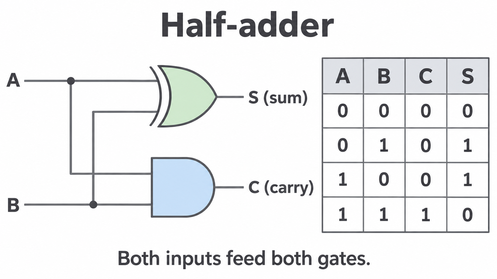
For A = 1, B = 1, XOR produces S = 0 and AND produces C = 1. Read the result in the order CS, giving 10, which represents two. For A = 1, B = 0, C = 0 and S = 1, giving 01. Carry and sum are separate wires; calling both of them “the output” obscures their different roles.
To construct the circuit in your notebook, draw one XOR and one AND. Branch A to one input of each gate and B to the other input of each. Mark the two actual branching junctions with dots, label the XOR output S and the AND output C. Do not connect the XOR output into AND: both gates receive the original input bits. The reference diagram has an unconnected wire crossing without a dot.
A half-adder has no input for an incoming carry. It is therefore insufficient by itself for a later column of a multi-bit addition when a previous column can carry into that column.
A full-adder includes an incoming carry
A full-adder combines two input bits with the carry from the preceding bit position.
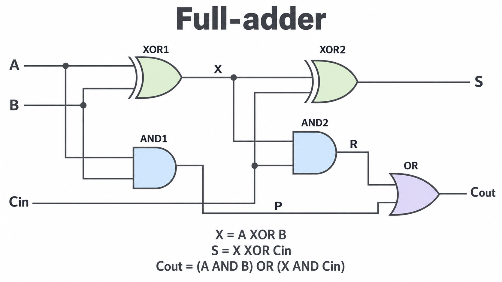
The inputs are A, B and ; the outputs are S and . One construction uses two half-adders and an OR gate. First set and . Then add X and , giving and . OR combines the two possible carry outputs: .
[DIAGRAM: asset_slug: full-adder; description: Two XOR stages form the sum; two AND outputs feed OR to form the outgoing carry. Junction dots mark connected branches.]
| A | B | S | ||
|---|---|---|---|---|
| 0 | 0 | 0 | 0 | 0 |
| 0 | 0 | 1 | 1 | 0 |
| 0 | 1 | 0 | 1 | 0 |
| 0 | 1 | 1 | 0 | 1 |
| 1 | 0 | 0 | 1 | 0 |
| 1 | 0 | 1 | 0 | 1 |
| 1 | 1 | 0 | 0 | 1 |
| 1 | 1 | 1 | 1 | 1 |
Trace A = 1, B = 0 and : X = 1 and P = 0; the second stage gives S = 0 and R = 1; OR gives . The result is 10, agreeing with 1 + 0 + 1 = 2. For 1 + 1 + 1, X = 0, P = 1, S = 1 and R = 0, so the result is 11.
Carry-out is 1 when at least two of the three input bits are 1. Sum is 1 when an odd number are 1. This is a useful check, but you should also be able to trace the actual gate connections. In a multi-bit adder, one column's carry-out feeds the next more significant column's carry-in.
Edge-triggered D-type memory
A stored bit must retain a value instead of changing whenever an input changes.
An edge-triggered D-type flip-flop stores one bit. D is its data input and Q is the stored output. A clock edge triggers an update: Q takes the value present at D at the specified active edge. The example here is rising-edge-triggered, so the active transition is clock 0 → 1. The small triangle on the clock input marks edge triggering; a clock-input inversion circle would indicate the opposite edge.
[DIAGRAM: asset_slug: d-type-memory; description: A rising-edge D-type unit copies stable D to Q at a 0-to-1 clock transition and retains Q between active edges.]
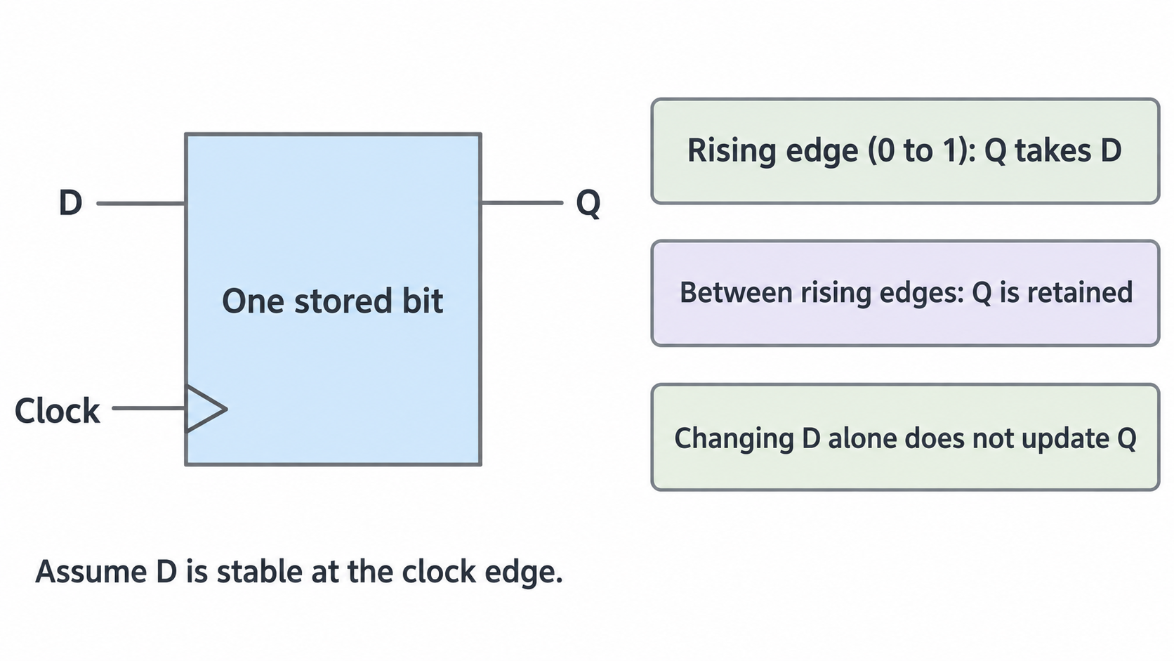
Between active edges, changing D alone does not change Q. Suppose Q initially equals 0. Set D to 1 while the clock stays 0: Q remains 0. On the next rising edge, Q becomes 1. If D then falls to 0 while the clock remains high, Q remains 1. A falling clock edge does not update this rising-edge unit; the next rising edge with D = 0 changes Q to 0.
Assume D is stable around each active edge in these idealised traces. Real devices have timing requirements, but analysing those timings or the internal gate construction is outside this specification's demand. The examinable idea is the unit's memory behaviour, not its internal operation.
Multiple such storage units can hold a multi-bit value, with one unit per bit. A shared clock allows the bits to be captured at the same active edge. This illustrates why a clocked memory unit differs from a combinational gate circuit: a gate's output follows its current inputs after propagation, whereas the flip-flop's output also depends on the previously stored state.