3.1.1 - Von Neumann architecture and fetch-decode-execute
A processor does not run a whole program in one leap: it moves one instruction through a precise sequence of small steps. In this lesson, you will follow those movements through RAM, CPU registers and buses, then explain how fetch, decode and execute work together. By the end, the names will describe a connected system rather than a list of mysterious boxes.
The stored-program concept
When a program is running, its instructions must be somewhere the processor can reach. In a von Neumann system, the program instructions and the data being processed are both held in the same main memory, normally RAM.
Von Neumann stored-program concept
Program instructions and data are stored in the same main memory, from which the CPU can fetch instructions and access data.
Each RAM location has an address, rather like a numbered locker. The contents at an address might be a program instruction or a piece of data. The CPU uses the address to request the required contents; RAM stores the contents but does not decode or carry out an instruction.
This simplified memory snapshot uses short, human-readable instruction descriptions. It is not an instruction-set format that you need to learn.
| RAM address | Contents | Role in this example |
|---|---|---|
| 40 | ADD value from address 52 | program instruction |
| 41 | STORE result at address 53 | program instruction |
| 52 | 6 | data |
| 53 | 0 | data space for a result |
The important relationship is visible in the table: addresses 40 and 41 contain instructions, while addresses 52 and 53 contain data, yet all four locations belong to the same RAM. The CPU can fetch an instruction from address 40 and later access the data at address 52 while carrying it out.
Do not reduce the idea to "the CPU and RAM are connected". The discriminating feature is that instructions and data share main memory. That is why an instruction can be stored, addressed and transferred just as other binary contents can be.
CPU components and registers
The central processing unit (CPU) carries out program instructions. In the GCSE model, its control unit, arithmetic logic unit and registers have different but cooperating jobs. RAM is main memory outside the CPU; registers are storage locations inside the CPU.
Control unit (CU)
The CPU component that coordinates the other components, decodes instructions and sends control signals so that the required operations happen in the correct order.
The control unit therefore acts as the coordinator for the cycle. A different component carries out arithmetic and logical work.
Arithmetic logic unit (ALU)
The CPU component that carries out arithmetic operations and logical operations such as comparisons.
The CU directs; the ALU calculates or applies logic. Saying that the CU "does all the processing" loses this distinction. The CU may tell the ALU what operation is required, but the ALU performs that arithmetic or logical operation.
Register
A small storage location inside the CPU that temporarily holds an address, instruction, data value or result currently needed by the processor.
A simplified CPU model names registers by the particular state each one holds:
| Register | Full name | What it holds |
|---|---|---|
| PC | program counter | the address of the next instruction to fetch |
| MAR | memory address register | the address of the RAM location currently being read from or written to |
| MDR | memory data register | the instruction or data being transferred to or from RAM |
| CIR | current instruction register | the fetched instruction while it is being decoded and executed |
| ACC | accumulator | a data value being processed or a result produced by the ALU |
Two pairs are easy to confuse. The PC contains an address, not the instruction itself; after fetching, the instruction is held in the CIR. The MAR answers "which location?", while the MDR answers "what contents are moving to or from that location?"
The clock produces regular timing pulses. These pulses synchronise the small transfers and operations directed by the CU, keeping components working in step. One pulse should not be treated as one complete instruction: fetching and carrying out an instruction involves several coordinated actions.
[DIAGRAM: asset_name: Von Neumann stored-program system; asset_slug: 3_1_1_von_neumann_architecture_and_fetch_decode_execute__diagram_01; recommended_method: image_gen; description: A monochrome 16:9 architecture diagram with the clock feeding timing pulses to the control unit, the control unit, ALU and PC/MAR/MDR/CIR/ACC registers nested inside the CPU, instructions and data sharing one RAM, and correctly directed address, data and control buses between CPU and RAM.]
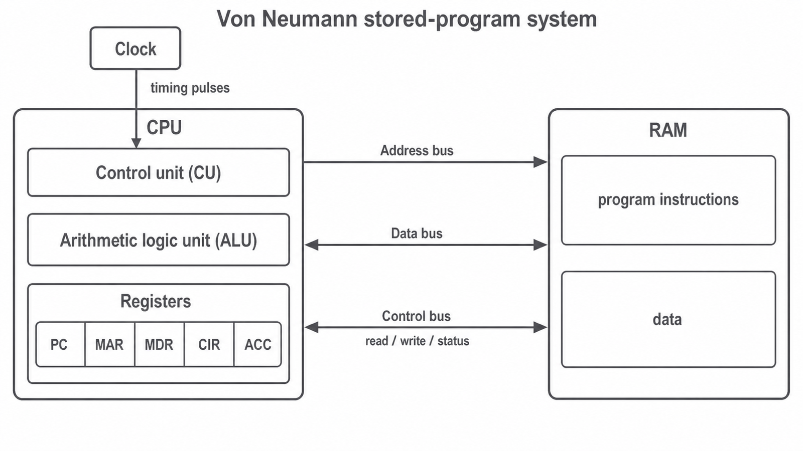
Consider a moment just after the instruction at address 40 has been fetched. The PC can already hold 41, ready for the following instruction, while the CIR holds ADD value from address 52. Those are not conflicting values: one is an address for the future fetch; the other is the instruction currently being handled.
The three system buses
A bus is a communication pathway made from a collection of connections that carry signals between computer components. The address, data and control buses connect the CPU and main memory, but they do not carry interchangeable messages.
| Bus | What it carries | Direction in this simplified model | Example during a memory read |
|---|---|---|---|
| Address bus | the address of a location | CPU to RAM | MAR supplies address 40 |
| Data bus | an instruction or data value | either direction | RAM returns the contents of address 40 to the MDR |
| Control bus | coordination signals, such as read, write and status signals | either direction overall | CU sends a READ signal to RAM |
Use three questions to keep their roles separate:
Continue this lesson.
You’re previewing NovaLearn without an account. Create a free account to read the rest.
Create free account